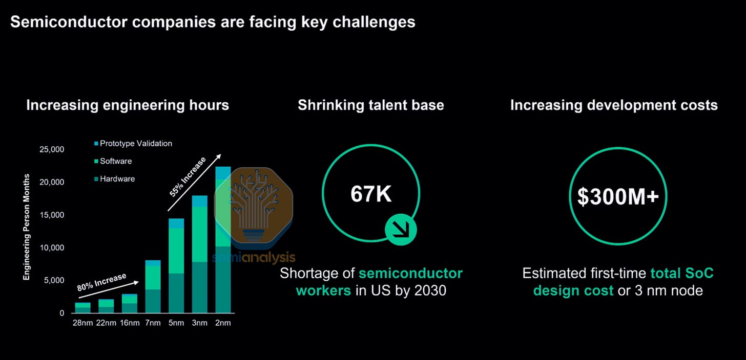
AI demand has been driving the explosion in compute over the past few years, resulting in chip designs getting ever more complex, with silicon area and power per package seeing continued growth as designs push for even greater performance. With each successive generation, new process nodes with more design rules and restrictions further increase chip design costs.
At the same time, the rush to bring compute into the market as quickly as possible has put design teams under immense pressure to compress timelines and speed up validation cycles from years to months. If you’re not fast, you will get lapped up and beaten by your competitors. Even a 3 month delay means billions of dollars.
Source: Siemens
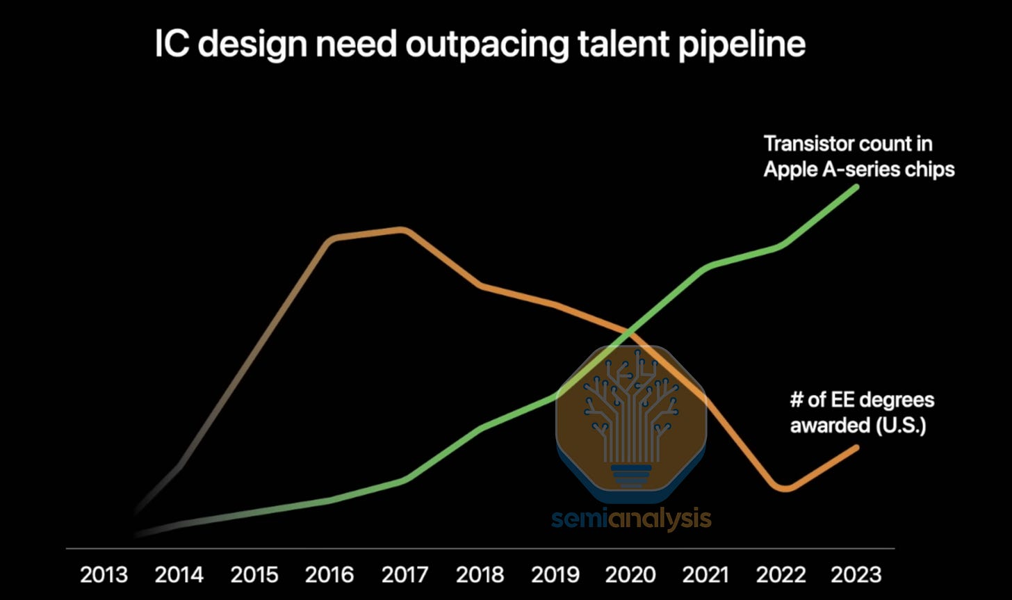
All this is happening while the engineering talent base is shrinking. Lucrative salaries and flexible working arrangements have enticed most students into the Software and Information Systems tracks, resulting in a dwindling number of Electrical Engineer graduates that could enter the chip design workforce. Siemens presented the engineer-hours demanded of these numerous complex AI accelerator designs that far outstrip the engineering talent coming into the workforce.
One-third of the current U.S. semiconductor workforce is over 55. The pipeline of new graduates is nowhere close to filling that gap. Even Apple is actively funding education programs to encourage uptake in engineering. While their New Silicon Initiative has contributed to increasing interest and number of EE graduates, it barely moves the needle compared to the explosion in manpower requirements as transistor count grows at a Moore’s Law pace.
Source: Apple
With this trifecta of increasing chip complexity, compressed design timelines and a shortage of engineers, a massive bottleneck has formed at the design stage. The latest AMD MI455X packs 320 billion transistors across 12 logic dies on 2nm and 3nm processes with advanced Hybrid Bonding 3D die stacking, HBM4 memory integration and high speed 224G SerDes. Designing something at this scale is not a matter of hiring more engineers or buying more verification servers. It tests a company’s tooling, methodology, and human capital organization as to whether the design succeeds or fails.
After spending hundreds of millions of dollars on a new SoC design, there is no guarantee the chip will work. Multiple steppings are usually required that need new mask sets, with A0 rarely going into production. When a single advanced mask set costs tens of millions of dollars, every respin is a gut punch to the balance sheet. Furthermore, it adds months to the schedule for high volume production start.
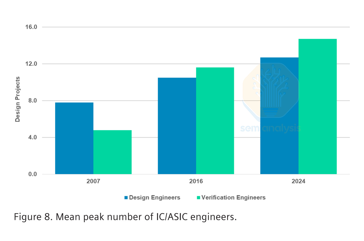
As designs get more complex, testing is becoming more important to ensure all modules within a chip are interoperable and locally sound. Verification, the process of proving a design does exactly what it should before committing it to silicon, now consumes up to 70% of total project effort, depending on the design. Verification engineers are the fastest-growing job category in chip development, and the industry still cannot hire them fast enough.
Source: Siemens
While chip complexity grows at roughly 50% per year, driven by new nodes and larger SoCs, design productivity improves only about 20% each year. This design productivity gap means every new generation of silicon demands exponentially more engineering effort, more compute, and more sophisticated automation.
The semiconductor industry’s ability to keep building more powerful chips depends not on physics or lithography alone, but on EDA (Electronic Design Automation) software. These tools effectively translate human intent into manufacturable silicon. Without EDA, no chip designed after the mid-1980s would exist.
This primer is your guide to EDA in the semiconductor industry. In this first part, we will walk the entire journey from RTL (Register Transfer Level) code, the high-level hardware description language that engineers actually write, all the way to manufactured, packaged silicon. We will name the tools, explain the tradeoffs, and show why EDA is one of the most consequential and underappreciated sectors in technology.
In part 2, our EDA Market Primer dives deep into the business of EDA, profiling the major companies (Synopsys, Cadence, Siemens) and their revenue and business models. We provide comprehensive market analysis and monitoring the Chinese EDA effort, as well as IP licensing and outsourcing to design partners and the transition to Customer Owned Tooling (COT) with hyperscaler ASIC designs.
Part 3 then assesses how AI is disrupting the EDA industry, covering the full gamut from startups and engineer dashboards to agentic chip design flows from NVIDIA and the big three. The concept of using AI accelerators to create superhuman designs that go into future AI accelerators is the most exciting development that our industry has seen in decades. Stay tuned as we cover the incoming revolution in chip design.
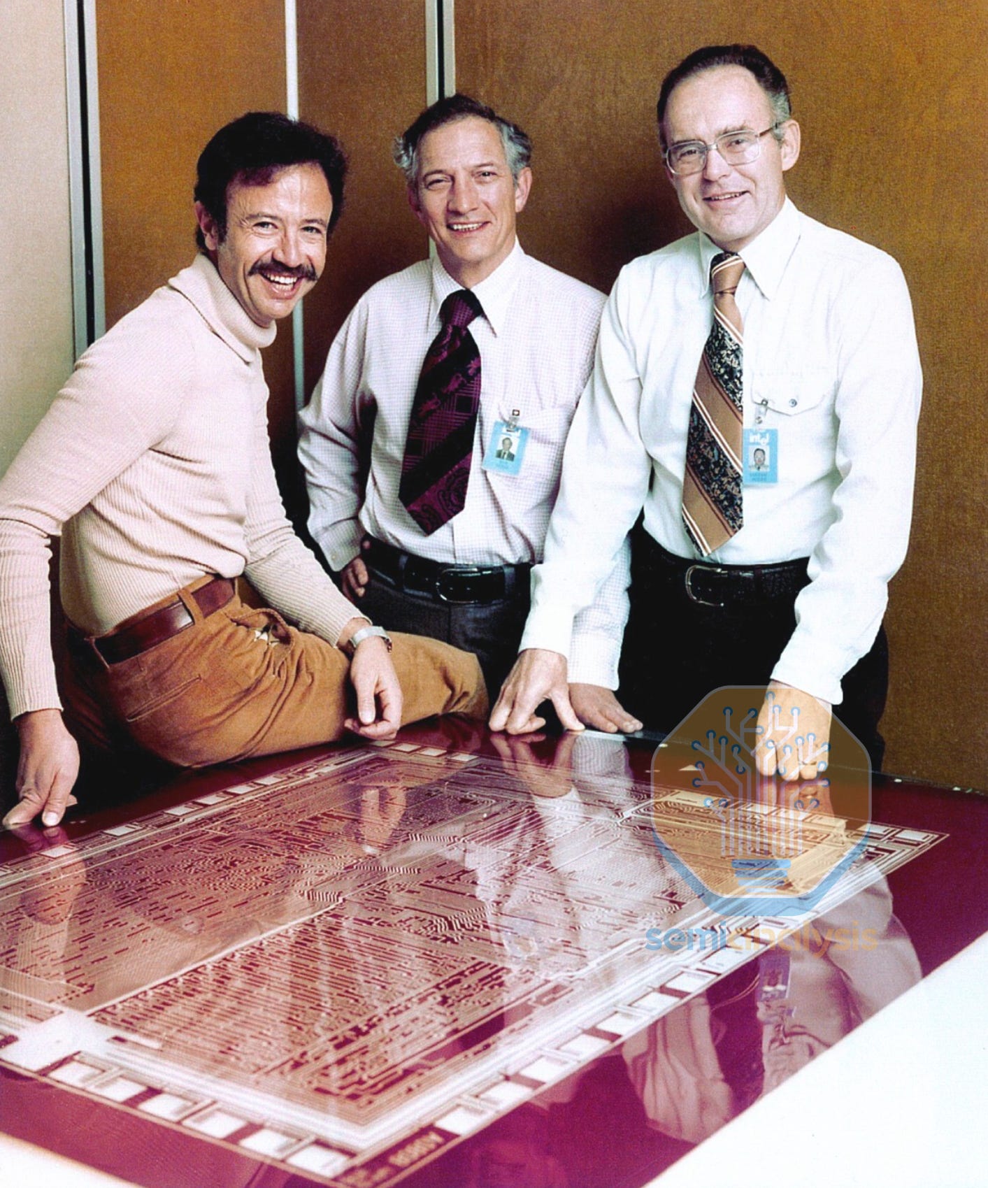
Source: Intel