Transistors. Integrated circuits. FET. CMOS. FinFET. Photolithography. EUV lithography. The United States invented all of the foundational technologies powering modern-day semiconductors.
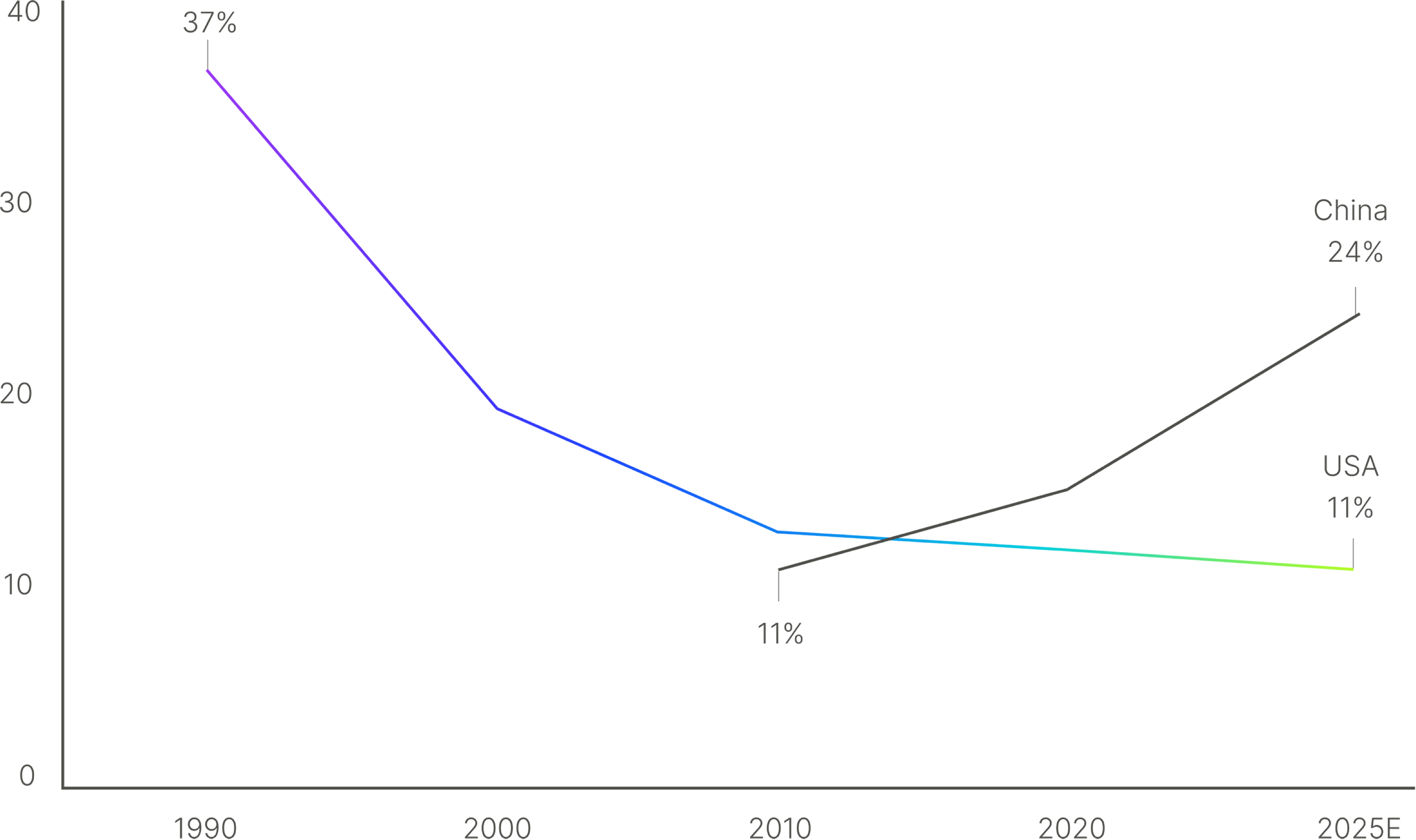
But over the past decade, the United States has lost the lead in semiconductor production and the most advanced parts of the supply chain.
Percent of global semiconductor fabrication capacity for 300 mm wafers
With today's explosion in artificial intelligence and robotics, the number of chips needed year over year is increasing exponentially. However, the number of chips we can produce is bottlenecked by the number of semiconductor fabs we have. At the same time, we face the challenge of China's rapid semiconductor progress and its plans to win the AI race against the United States.
The rising costs to build and outfit advanced semiconductor fabs, coupled with critical gaps in our domestic supply chain, are preventing us from realizing the full potential of returning America to dominance in semiconductor production.
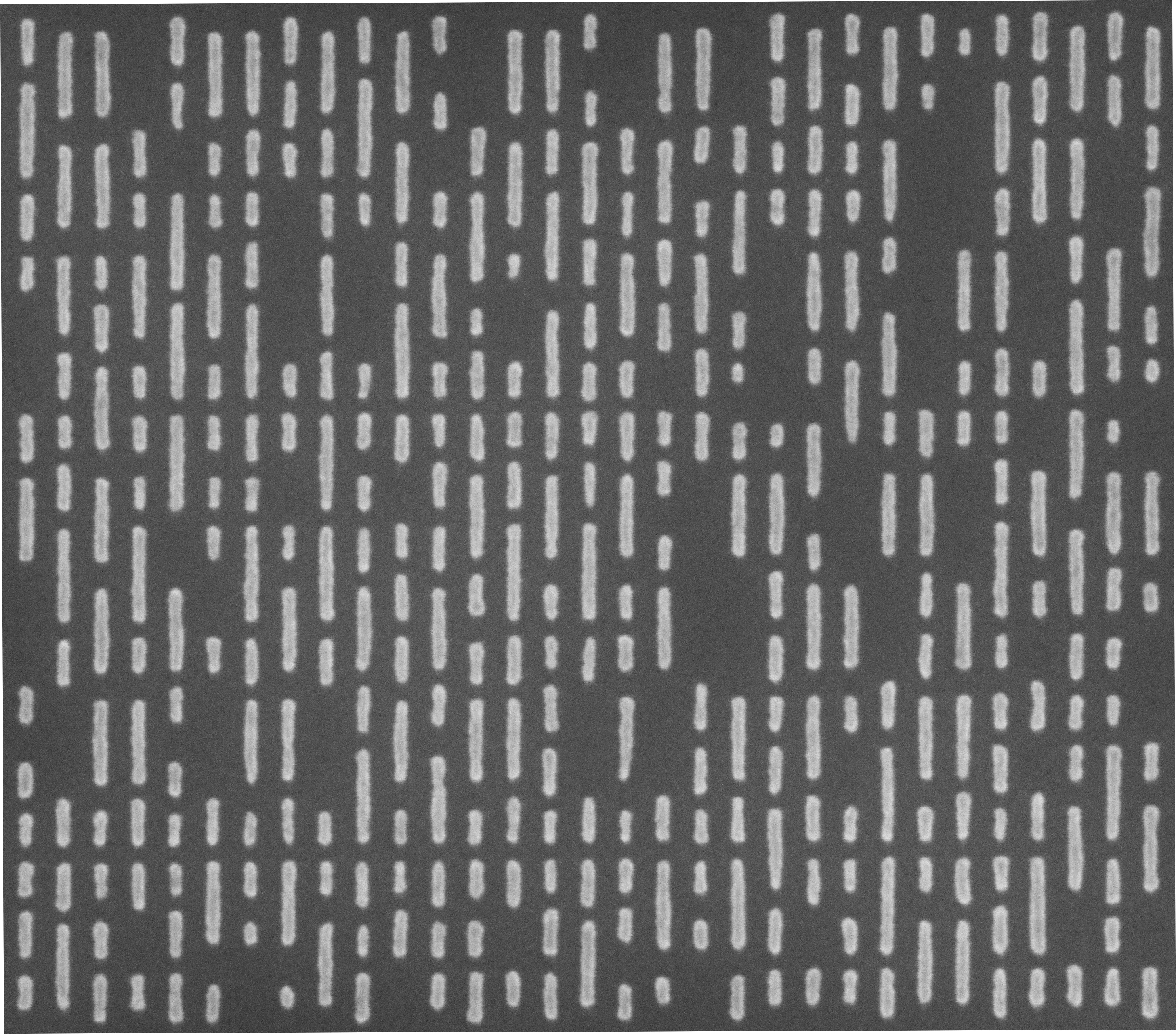
Random logic contact array of 12 nm critical dimensions and 13 nm tip-to-tip spacing printed with high pattern fidelity.
Substrate was founded to return the United States to dominance in semiconductor fabrication on three core beliefs:
To achieve this, Substrate is building next-generation semiconductor fabs to return America to dominance in semiconductor production and will use our technology—a new form of advanced X-ray lithography—to power them.
Our results shown here can be compared with the current industry's "high numerical aperture" (High NA) EUV lithography and are equivalent in resolution to the 2 nm semiconductor node, with capabilities to push well beyond.
To accomplish this, we had to invent a new technology capable of producing the critical patterns required for today's advanced silicon, which was lower cost, less complex, more capable, and faster to build.
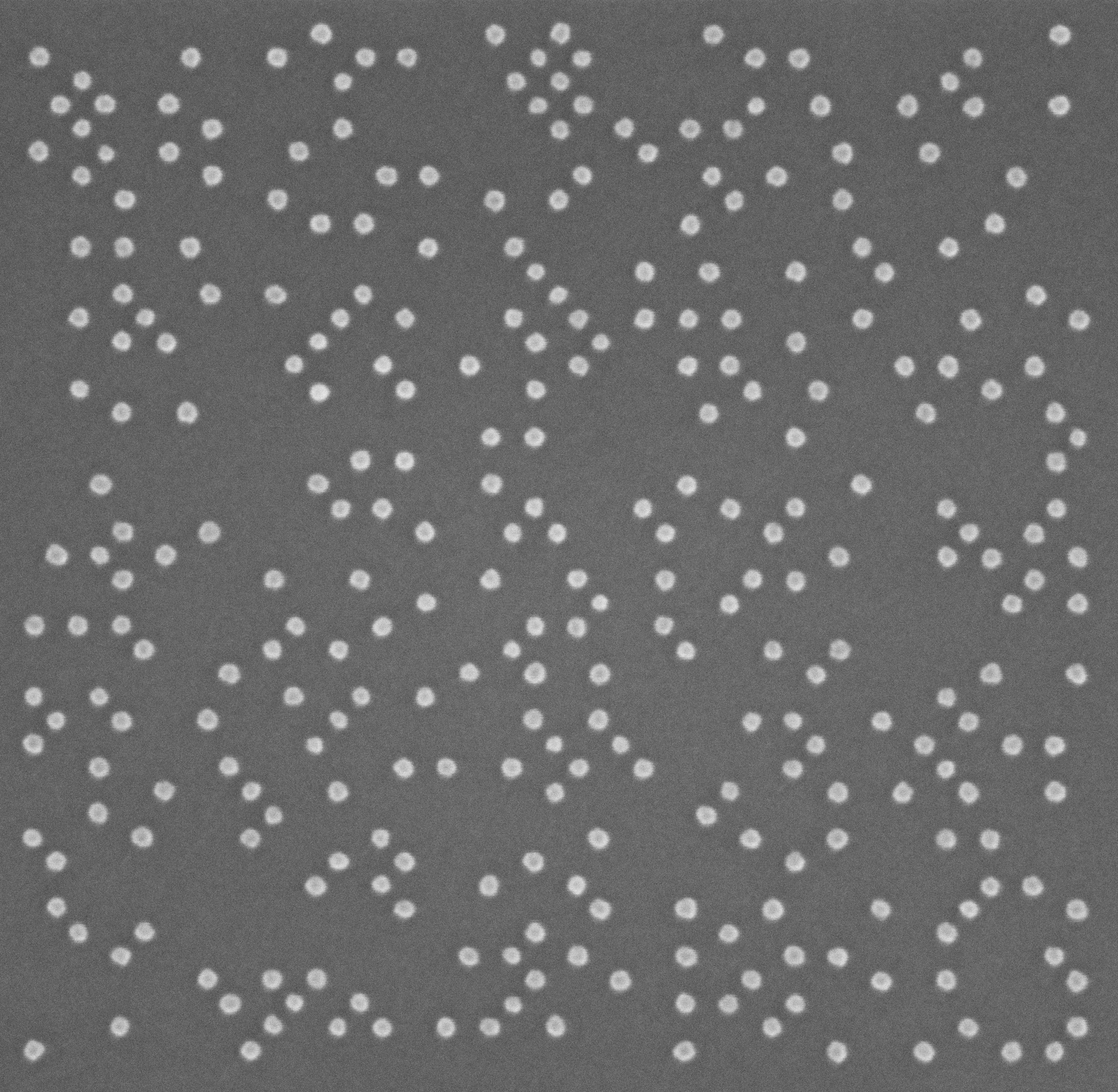
Random vias with 30 nm center-to-center pitch with superb pattern quality and critical dimension uniformity.